Thin film deposition surface layer.
Thin film deposition is the process of generating a very thin coating of material onto another thicker substrate material.
Thin film layers of different materials are built up using masking techniques to create electronic devices on the surface of the base material.
This leads to a highly stable miniature electronic component which retains the mechanical properties of the substrate material.
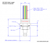
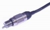
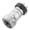
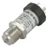
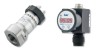
Featured thin film sensor technology related products
Related Technical Terms
- BFSG – Bonded Foil Strain Gauge
- Bourdon Tube
- Capacitive Fluid Level Measurement
- Ceramic Pressure Sensors
- Conductive Fluid Level Detection
- Doppler Effect Flow Measurement
- Float Fluid Level Detection
- LVDT – Linear Variable Differential Transformer
- Paddle Wheel Sensor
- Piezoresistive Strain Gauges
- Positive Displacement Flow Measurement
- Pressure Transducers
- Radar Distance Sensing
- SOI – Silicon on Insulator
- Strain Gauge
- Transit Time Flow Measurement
- Turbine Rotor Sensor
- Ultrasonic Distance Sensing
- Ultrasonic Flow Velocity Sensors
- Vibrating Tuning Fork Fluid Level Detection
- Vortex Flow Measurement
- Wheatstone Bridge Strain Gauge